
Thin-Film Solar Panel Manufacturing Processes
In the dynamic landscape of solar energy, thin-film solar panels have emerged as a promising alternative to traditional crystalline silicon modules. The pursuit of more efficient, cost-effective, and versatile photovoltaic technologies has led to significant advancements in thin-film manufacturing processes. As discussions about “best solar companies in VA” gain momentum, understanding the intricacies of thin-film production is crucial for stakeholders in the solar industry to get best solar companies in VA.
Introduction to Thin-Film Solar Panels
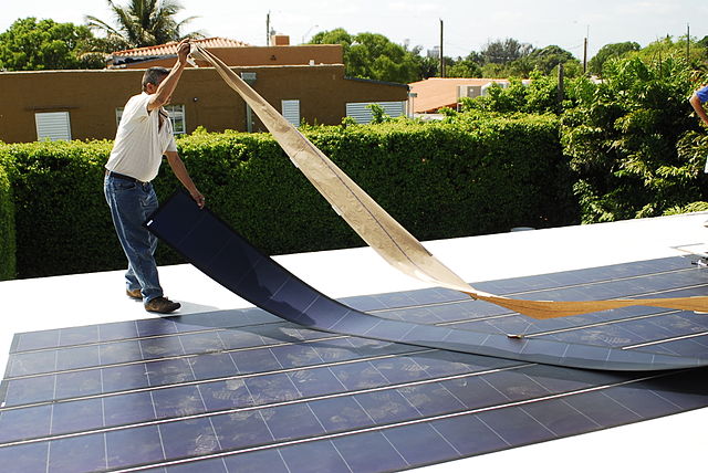
Thin-film solar panels represent a category of photovoltaic modules characterized by their thin, flexible, and lightweight design. This innovative technology offers distinct advantages over conventional crystalline silicon panels, driving its adoption in residential, commercial, and utility-scale solar projects.
Overview of Thin-Film Technology
Thin-film solar panels are composed of one or more thin layers of photovoltaic material deposited onto a substrate, typically glass or flexible plastic. These panels exhibit higher flexibility and lower weight compared to crystalline silicon modules, making them suitable for a diverse range of applications, including building-integrated photovoltaics (BIPV) and portable electronics.
Different Types of Thin-Film Solar Panels
Several types of thin-film solar technologies exist, each utilizing different semiconductor materials to generate electricity from sunlight. Amorphous silicon (a-Si), cadmium telluride (CdTe), and copper indium gallium selenide (CIGS) are among the most commonly used materials in thin-film manufacturing, each offering unique performance characteristics and production processes.
Importance of Manufacturing Processes
The manufacturing processes employed in thin-film solar panel production play a pivotal role in determining the efficiency, durability, and cost-effectiveness of the final product. Innovations in deposition techniques, layering, encapsulation, and quality control have contributed to the evolution of thin-film technology and its competitiveness in the solar market.
Manufacturing Processes for Thin-Film Solar Panels
Thin-film solar panel manufacturing involves a series of intricate processes aimed at depositing semiconductor layers, encapsulating the cells, and ensuring quality control throughout the production cycle.
Deposition Techniques
Deposition techniques are used to deposit thin layers of semiconductor material onto the substrate, forming the active photovoltaic layers of the solar panel.
Chemical Vapor Deposition (CVD)
Chemical vapor deposition involves the chemical reaction of precursor gases to deposit thin films of semiconductor material onto a substrate. This process allows for precise control over film thickness and composition, facilitating the production of high-quality thin-film solar cells.
Physical Vapor Deposition (PVD)
Physical vapor deposition methods involve the physical evaporation of semiconductor materials followed by condensation onto the substrate. Techniques such as sputtering and evaporation are commonly used to deposit thin films of materials like CdTe and CIGS onto glass or flexible substrates.
Solution-Based Deposition
Solution-based deposition techniques involve the deposition of semiconductor materials from liquid solutions or suspensions onto the substrate. Methods such as inkjet printing and spin coating offer scalability and cost-effectiveness, particularly for flexible and lightweight thin-film solar panels.
Layering and Encapsulation
Once the semiconductor layers are deposited, additional layers are added to enhance conductivity, transparency, and durability, while encapsulation protects the cells from environmental degradation.
Semiconductor Layer Deposition
Additional layers, such as transparent conductive oxides (TCOs) and metal contacts, are deposited to facilitate electron flow and maximize light absorption. These layers are critical for optimizing the efficiency and performance of thin-film solar cells.
Transparent Conductive Oxide Layer
Transparent conductive oxide layers, such as indium tin oxide (ITO) or fluorine-doped tin oxide (FTO), serve as transparent electrodes that allow sunlight to reach the semiconductor layers while facilitating the extraction of generated electricity.
Encapsulation for Protection
Encapsulation materials, such as ethylene-vinyl acetate (EVA) or glass, are used to seal the solar cells and protect them from moisture, temperature fluctuations, and mechanical stress.